A major technological challenge is the finding of a new material for the postsilicon post-silicon CMOS era. Graphene exhibits the excellent properties of carbon nanotubes (CNT), while not suffering from placing and scalability problems. Epitaxial graphene is the most viable candidate for high-speed low power nano-electronics device applications as recognized by the industry. An almost unexplored avenue for graphene is ballistic nanoelectronics. Pristine CNTs are known to be ballistic conductors even at RTroom temperature and to withstand high current densities. Graphene ribbons nanoribbons are predicted to have similar properties and are thus interesting for all-graphene circuitry, for they are claimed to have better mobility and stand higher current densities than Cu wires.. However most strategies involve the growth of extended graphene 2D sheets and subsequent graphene nano-patterning that degrades considerably the electronic mobility of nanopatterned graphene.
The CoRiGraph project focuses on graphene nanostructures produced Graphene nanoribbons can be produced in epitaxial graphene by non‐lithographic techniques on the sidewall of pre-etched SiC steps silicon carbide. This technique takes full advantage of the single crystalline SiC substrate. It is scalable as already demonstrated by the fabrication of 10,000 transistors on a single chip. Moreover, transport data suggest Nanoscopic ribbons have been shown to have remarkable properties. A gap is observed on the graphene ribbon edge and ballistic transport is demonstrated. This suggests smooth edges since disordered-related effects (localization, transport gap) are not observed. These ribbons may be the needed breakthrough in graphene electronics, opening new possibility of ballistic transport, non linear effect in ballistic junctions and new all-graphene interconnects. This opens the way for electronics based on ballistic transport and coherent effects, which cannot be realized in with conventional semiconductors.
The primary goal of this the CoRiGraph project is thus to study the atomic and electronic structure of graphene nanoribbons grown on SiC sidewalls, and compare them with lithographically etched ribbons. Metal contacts on graphene, a key issue to any device fabrication will be also studied. The main objective of CoRiGraph project is to study open questions on graphene sidewall nanoribbons and on metal/graphene interfaces about their atomic and electronic structure, which can be properly addressed with the These questions will be addressed by a complementary set of experimental techniques (ARPES, STM/STS, STEM) and calculations theoretical studies (quantum transport) available at the consortium.put together in the consortium.
The CoRiGraph project is funded by the French National Research Agency.
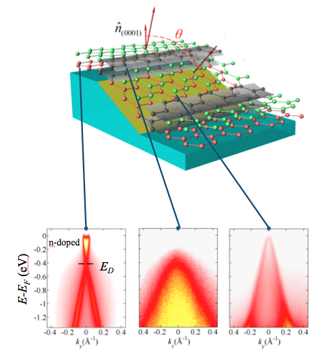
Highlight: a metal-semiconducting-metal all graphene nanostructure on graphene sidewall ribbons
Preliminary results on these ribbons are very promising. Photoemission has allowed us to observe that at the edge of these graphene strips, a semiconductor, is bonded to metallic graphene. This semiconductor is only a few nanometers wide (a few graphene lattice constants), a level of precision beyond modern lithographic limits.
To learn more:
« A wide band gap metal-semiconductor-metal nanostructure made entirely from graphene ».
J. Hicks, A. Tejeda, A. Taleb-Ibrahimi, M.S. Nevius, F. Wang, K. Shepperd, J. Palmer, F. Bertran, P. Le Fèvre, J. Kunc, W.A. de Heer, C. Berger, et E.H. Conrad.
Nature Physics 9, 49 (2012). Link to article.


